Introduction to LAM technology
LAM technology, namely Laser Activation Metallization, is a technology that uses lasers to make conductive circuits on insulating substrates such as ceramics. LAM technology uses high-energy laser beams to ionize ceramics and metals, so that they are firmly combined to form conductive circuits. LAM technology has the advantages of high resolution, good conductivity, and multiple welding. It is one of the key technologies for realizing three-dimensional interconnected devices.
Application of LAM technology in circuit board manufacturing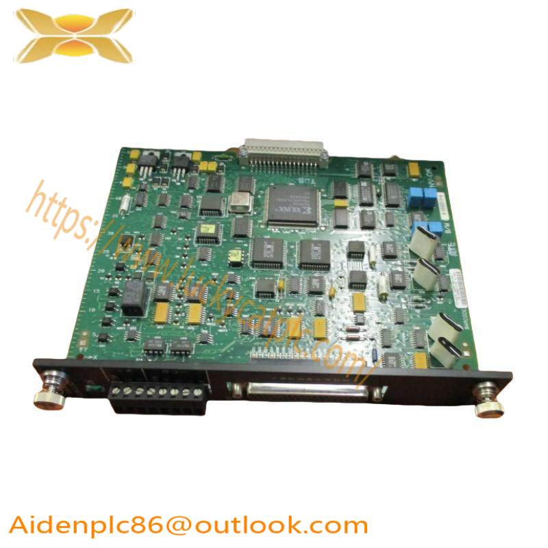
Improve the performance of circuit boards: LAM technology can produce circuit boards with excellent high temperature resistance, electrical insulation performance and chemical stability, which are suitable for fields with high requirements for use temperature, humidity and reliability.
Realize three-dimensional circuits: LAM technology can easily realize three-dimensional circuits, and fine resolution can manufacture complex circuit pattern structures to achieve more functions and higher integration.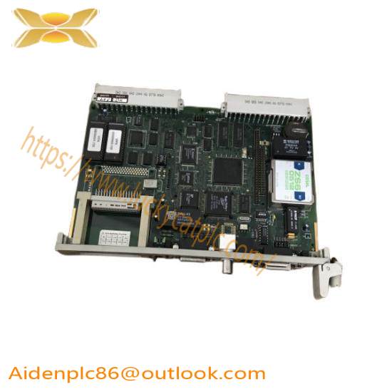
Reduce the number of installation levels and components: Three-dimensional interconnected devices prepared by LAM technology can choose appropriate shapes according to design needs, reduce the number of installation levels and components, and reduce production costs.
High bonding strength: LAM technology can form a strong bond between the metal layer and the ceramic, ensuring the stability and reliability of the circuit board.
Excellent conductivity: The conductive lines made by LAM technology have good conductivity and can meet the current transmission needs of various electronic devices.
High precision: LAM technology has fine resolution and can easily manufacture complex circuit pattern structures to achieve fine circuit layout and routing.
Multiple welding capabilities: Circuit boards made by LAM technology can withstand multiple welding operations and are suitable for various complex electronic assembly processes.
Laser activation: LAM technology activates the surface of the substrate through a laser beam, allowing it to combine with metal ions to form a strong metallization layer.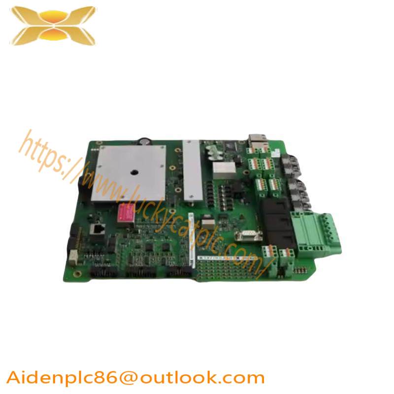
Application scenarios
Circuit boards using LAM technology have broad application prospects in many fields, including but not limited to:
Military industry, aviation, and aerospace: These fields have extremely high requirements for high temperature resistance and high reliability of circuit boards, and ceramic circuit boards made by LAM technology can meet these requirements.
Automobile: With the increasing degree of automotive electronics, the requirements for circuit boards are also getting higher and higher. Circuit boards made by LAM technology can be used in automotive control systems to improve the stability and reliability of the system.
Industry: In industrial control systems, circuit boards also play an important role. Circuit boards made with LAM technology can be used in industrial control systems to improve the accuracy and reliability of the system.
Communication: In the field of communications, circuit boards are an important part of communication equipment. Circuit boards made with LAM technology can be used in communication equipment to improve the performance and stability of the equipment.






There are no reviews yet.